
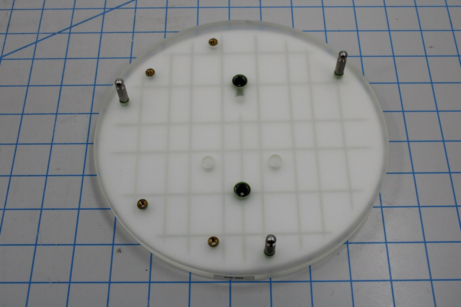
Introduction to the basic concept, working principle and application fields of Wafer ChuckI. Introduction Wafer chuck is an important tool used in semiconductor manufacturing, optical processing, flat
Read More..
Preface:The semiconductor industry is the mainstay of the global high-tech manufacturing industry, and the quality and stability of its products are related to the technological development of modern
Read More..
Precision machining mechanical door linkage in the application of semiconductor equipmentI. IntroductionSemiconductor is one of the basic materials in modern electronics industry and an important mate
Read More..![[GPM Share]High Precision Injection Molding Process: A New Era of Precision Injection Molding](/uploadfiles/2023-04/16819885282298414.jpg)
I. Introduction:High-precision injection molding technology is a high-precision, high-quality, high-efficiency, low-cost injection molding technology that has been widely used in medical devices, opti
Read More..![[GPM Share]ESC static suction cup: history, application, and technology](/uploadfiles/2023-04/16818829223365461.png)
ESC electrostatic suction cups: invention history, applications and technological directions, market demands and development trends ESC electrostatic suction cups are equipment widely used in the indu
Read More..
The MOCVD (metal organic chemical vapor deposition) technology in semiconductor material growth has extensive applications in modern electronics and optoelectronics. The main advantage of MOCVD techno
Read More..
Foreword:Semiconductor devices are one of the most important devices in todays electronic technology field. In the semiconductor chip manufacturing process, the reaction chamber is a crucial comp
Read More..![[GPM Share] Challenges and Future Development Trend Analysis of Semiconductor Equipment Parts Maintenance and Manufacturing](/uploadfiles/2023-04/16814798938579710.jpg)
With the rapid development of the semiconductor industry, the manufacture and maintenance of semiconductor equipment components has become an indispensable link in the semiconductor industry. However,
Read More..![[GPM Share]Precision Manufacturing of Semiconductor Electron Beam Lithography Equipment and Its Vacuum System](/uploadfiles/2023-04/16812044596014539.jpg)
One. IntroductionSemiconductor electron beam lithography equipment is an indispensable tool in todays microelectronics manufacturing process. Its appearance has greatly promoted the improvement o
Read More..![[GPM Share] The History, Principles and Parts Manufacturing of Physical Vapor Deposition Equipment PVD](/uploadfiles/2023-04/16811087879103346.png)
Physical vapor deposition equipment, referred to as PVD equipment, is a technology that uses physical methods to evaporate or sputter materials from the source to the surface of the substrate for thin
Read More..